HKUST Engineering Researchers Developed a Novel Photodetector to Enhance Performance of On-Chip Light Monitoring
, Head and Professor of the Department of Electronic and Computer Engineering at HKUST, and PhD student Niu Yue (right) at the Photonic Device Laboratory.")
Programmable photonics promise faster and more energy-efficient computing than traditional electronics by using light to transmit signals. However, current systems are limited by the need for precise on-chip power monitors. Researchers from the School of Engineering at The Hong Kong University of Science and Technology (HKUST) have developed a germanium-ion-implanted silicon waveguide photodiode. This novel photodetector achieves high responsivity, ultra-low optical loss, and minimal dark current, significantly enhancing the performance of on-chip light monitoring. It provides core hardware for energy-saving and ultra-sensitive biosensing systems, facilitating practical applications in programmable photonics. The findings have been published in the international journal Advanced Photonics.
Programmable photonic devices, which utilize light to perform complex computations, are emerging as a key area in integrated photonics research. Unlike conventional electronics that transmit signals using electrons, these systems employ photons, offering faster processing speeds, higher bandwidths, and greater energy efficiency. These advantages make programmable photonics particularly well-suited for demanding tasks such as real-time deep learning and data-intensive computing.
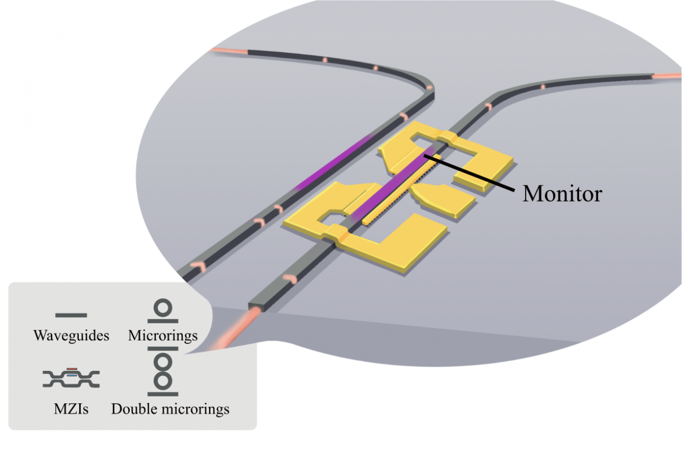
On-chip power monitors are core components for building programmable photonic networks, as their performance directly determines the system’s adaptive adjustment accuracy, stability, and effectiveness. However, existing photodetectors designed for this purpose face a fundamental trade-off. They have to maintain extremely low optical absorption loss to prevent significant attenuation of transmitted optical signals, and require high responsivity to detect weak optical power, along with low dark current and minimal power consumption.
To address these challenges, a team led by Prof. Andrew POON, Head and Professor of the Department of Electronic and Computer Engineering at HKUST, along with PhD student NIU Yue, has developed a germanium-ion-implanted silicon waveguide photodiode. This approach overcomes the challenges faced by existing on-chip power monitors, which struggle to balance responsivity and loss. The waveguide photodiode is a small light detector that can be integrated directly into an optical waveguide, which confines and transports light. Its primary purpose is to convert a small portion of the light traveling through the waveguide into an electrical signal that can be measured using conventional electronics. One way to enhance this conversion is through ion implantation, a process that introduces controlled defects into the silicon structure of the photodiode by bombarding it with ions. When executed properly, these defects can absorb photons with energies that are too low for pure silicon, thereby enabling the photodiode to detect light across a broader range of wavelengths.
Previous attempts to construct such detectors utilized boron, phosphorus, or argon ions. While these approaches improved performance in various aspects, they also introduced free carriers into the silicon lattice, which degraded optical performance. In contrast, the team opted to implant germanium ions. As a Group IV element like silicon, germanium can replace silicon atoms in the crystal structure without introducing a significant number of free carriers. This substitution enables the device to enhance its sensitivity without compromising signal quality.
The researchers conducted a series of comparative experiments to evaluate the performance of the new device. The results indicated that the germanium-ion-implanted photodiode exhibited high responsivity in both the 1,310 nm (O-band) and 1,550 nm (C-band), which are two critical wavelengths used in telecommunications. It also demonstrated an extremely low dark current, resulting in minimal unwanted output in the absence of light, as well as low optical absorption loss. This combination of features makes the device well-suited for integration into photonic circuits without disturbing the primary signal flow.
Prof. Andrew Poon stated, “We benchmarked our results against other reported on-chip linear photodetector platforms. The findings show our devices outperformed other platforms across key performance metrics for on-chip power monitoring. This study brings transformative potential of light-based computing closer to reality and represents a significant step toward practical, large-scale programmable photonic systems.”
Beyond its immediate use in programmable photonics, the new detector’s unique characteristics also open doors to other promising applications. Prof. Poon added that the detector’s ultra-low dark current and low bias voltage position it as an ideal candidate for energy-efficient, ultra-sensitive biosensing platforms, where low-noise detection of weak optical signals is paramount. This capability allows for direct integration with microfluidics in lab-on-chip systems, thereby fostering future applications in biosensing and lab-on-a-chip technologies.
(This news was originally published by the HKUST Global Engagement and Communications Office here.)