HKUST Researchers Develop Technology to Extend the Horizon of Wide-Bandgap Semiconductor Gallium Nitride Electronics
 and his team that developed this work.")
A research team led by Prof. Kevin CHEN of Department of Electronic and Computer Engineering at the Hong Kong University of Science and Technology (HKUST) has recently inducted a new member, the complementary logic circuitry, into the family of wide-bandgap gallium nitride (GaN) electronics, thereby substantially extending the horizon of the GaN research realm. The functionality and performance of GaN-based electronic devices and integrated circuits are expected to be further improved and become more competitive.
GaN-based electronic devices have been intensively researched and developed for more than two decades by both academia and semiconductor industry, and they have been recently commercialized and adopted in 5G wireless base stations, ultra-compact fast chargers for mobile devices and LiDAR systems. GaN-based power converters/supplies with unprecedented efficiency and power density are expected to see near-term adoptions in many emerging applications such as data centers, autonomous driving, electric vehicles, drones, robots, etc. All of these are power-hungry and yet demand ultra-compactness in power supplies. Wide-bandgap semiconductor GaN-based power electronics could meet these requirements much better than the conventional silicon-based counterparts. To unlock the full potential of GaN-based power systems with enhanced intelligence, reliability, and stability, a robust technology platform that allows integration of power switches and peripheral functional blocks including the ubiquitous logic circuits, has been pursued in the last decade.
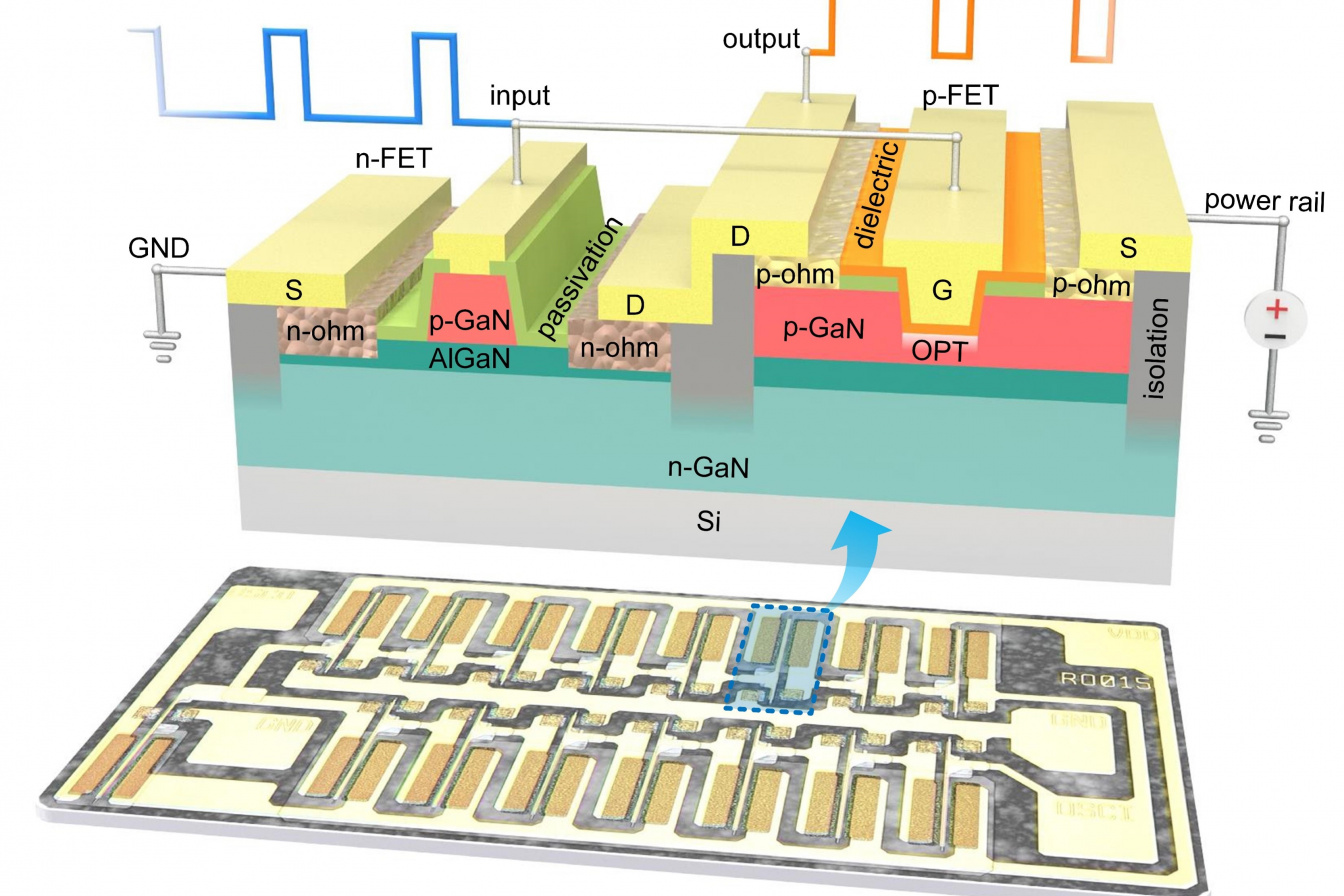
Complementary logic integrated circuits (ICs) are the foundation and dominant architecture in silicon microelectronics industry, which currently accounts for more than 90% of the semiconductor market. Complementary (or coined with a more popular term, CMOS) logic gates feature two different kinds of transistors (i.e., n-channel and p-channel) controlled by opposite logic that enables extremely low power consumption as one of the transistors is always turned off at either logic “1” or “0”. Development of the energy-efficient GaN CMOS technology has been slow until recently, as hindered by the difficulties in implementing p-channel transistors and integrating them with complementary n-channel ones.
On a GaN power device technology platform, Prof. Chen’s team developed a new approach to tackle a notorious problem associated with the gate-dielectric/channel interface. They engineered a “buried channel” structure enabled by an oxygen plasma treatment (OPT) technique, consequently realizing p-channel GaN transistors with well-balanced performance matrix of threshold voltage for enhancement-mode operation, high ON/OFF current ratio, and high current driving capability. Monolithic integration process was also developed to realize GaN CMOS ICs that are seamlessly integrated with GaN power switching devices.
For the first time, the team demonstrates a complete set of GaN CMOS-based elementary logic gates including NOT, NAND, NOR gates, and the transmission gate. The team also demonstrated multiple-stage logic circuits that can be operated at megahertz frequencies. “This is an exciting leap forward. We have first proven that all building blocks are functional, then these building blocks could be put together for more complicated entities. Therefore, any GaN-based complementary logic circuits can be constructed by making combinations of these logic gates,” says Prof. Chen.
Circuit designers can now start to design more powerful GaN ICs with more sophisticated functions. These ICs include, but are not limited to: 1) energy-efficient power ICs with advanced control, sensing, protection, and drive functions in addition to the basic power switching functions; 2) computing/control electronics for harsh environments such as in automotive and aviation systems. In the near-medium future, it becomes feasible to build GaN computing chips for critical missions such as planetary and deep space explorations.
The device technology in the work was developed at HKUST’s Nanosystem Fabrication Facility (NFF) on Clear Water Bay campus. The work is partially supported by a Hong Kong RGC Research Impact Fund (RIF) project and has recently received funding support from Shenzhen-Hong Kong-Macau Science & Technology Program. This work has recently been published in Nature Electronics.
(This news was originally published on EurekAlert on Aug 19, 2021.)